Perovskite-based solar cells, widely considered as successors to the currently dominant silicon cells, due to their simple and cost-effective production process combined with their excellent performance, are now the subject of in-depth research.
A team of scientists from the Fraunhofer Institute for Solar Energy ISE and the Faculty of Physics at the University of Warsaw presented perovskite photovoltaic cells with significantly improved optoelectronic properties in the journal Advanced Materials Interfaces. Reducing optical losses in the next-generation cells, as shown in the paper, is one of the key challenges for their broader implementation.
Photovoltaics has experienced a significant development over the past 20 years, considering both panel efficiency and the installed capacity, which has increased worldwide by a staggering 1000 times since year 2000.
Silicon has been the most commonly used material for producing photovoltaic panels, yet currently cells based on this element are approaching their physical efficiency limits. Therefore, scientists are actively exploring innovative solutions targeted at enhancing cell efficiency and simultaneously enabling cheaper and more environmentally friendly production.
Perovskite-based cells meet both of these criteria, offering efficiency above 26%, ease and cost-effectiveness in production using well-established chemical methods. Currently, numerous research institutes worldwide are working on improving their efficiency and resistance to atmospheric conditions. One of the challenges they are facing is the integration of perovskite cells with silicon cells while simultaneously reducing losses from reflection and parasitic absorption.
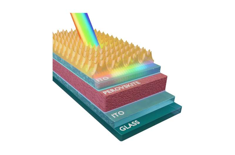
To minimize these losses, silicon cells are typically etched with highly corrosive chemical agents, a process that creates microscopic pyramid pattern on the surface, effectively reducing the reflection of the entire device, thereby increasing the current generated by the device. Unfortunately, perovskites are sensitive to many chemical substances, which is why less effective planar anti-reflective coatings applied through less invasive sputtering have been employed so far.
In research published in Advanced Materials Interfaces, scientists used the nanoimprinting method to create an efficient anti-reflective structure with honeycomb-like symmetry atop the perovskite solar cell. This technique allows the production of nanometer-scale structures on very large surfaces, exceeding 100 cm².
"This approach guarantees scalability in the production process of large-surface devices, which is crucial in the context of the urgent need for energy transformation toward renewable energy sources," says Maciej Krajewski, a researcher from the Faculty of Physics at the University of Warsaw. Such modified samples demonstrate higher efficiency compared to cells using previously employed planar anti-reflective layers.
In addition to enhancing efficiency, another significant finding from the published work is that the application procedure for this layer does not damage the perovskite, opening the possibility of using other structures tailored to the specific cell architectures. Until now, scientists applied similar anti-reflective structures as separately prepared layers, which were transferred in another technological process that was inevitably small-scale and susceptible to damaging the active layer.
By employing the direct nanoimprinting method, it becomes possible to manufacture the entire device on a large scale and in a single technological process, which is crucial for reducing the overall device costs.
Furthermore, the applied method is compatible with a tandem configuration, i.e., combining silicon and perovskite cells, opening up an entirely new possibilities for its application. Consequently, there is the potential for directly transferring the procedure to emerging photovoltaic architectures, which could lead to further improvements in efficiency. The published results pave the way for new photovoltaic devices with outstanding optoelectronic properties, utilizing nanoimprinting techniques in their production.